Pos:
Home KnowledgeTechnologyHigh thermal conductivity diamond wafer-based GaN, giving you excellent heat dissipation effect!The power electronics industry has seen the theoretical limits of silicon MOSFETs and now needs to move to new components. GaN-based high electron mobility transistor (HEMT) devices with superior electrical properties make them an effective alternative to MOSFETs and IGBTs in high voltage and high switching frequency motor control applications. GaN is a wide bandgap (WBG) material. Therefore, its bandgap (corresponding to the energy required for electrons to pass from the valence band to the conduction band) is much more forbidden than in silicon: in fact, it is about 3.4 electron volts, and 1.12 eV of silicon. With so much energy required, GaN requires a material 10 times thinner than silicon to block specific voltages, making the device more compact. The higher electron mobility of GaN HEMT leads to faster switching speed, as the charge normally accumulated in the joint can be dispersed more quickly. The faster the rise time, the lower the drain-source on-resistance (RDS(on)), and the lower gate and output capacitance that GaN can achieve, all contribute to its low switching losses and ability to operate at 10 times higher switching frequencies than silicon. Reduced power losses bring additional benefits such as more efficient power distribution, less heat generation, and a simpler cooling system.
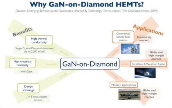
At the same time, the performance and reliability of GaN is related to the temperature and Joule heating effects on the channel. Substrates such as SiC and diamond integrated into GaN improve thermal management. This makes it possible to reduce the operating temperature of the device. For GaN-on-SiC devices, a 25-degree decrease in channel temperature results in approximately 10-fold increase in device lifetime. Diamond, on the other hand, has 14 times the thermal conductivity and 30 times the electrical field resistance. High thermal conductivity allows heat to be dismissed. The diamond has a band gap of 5.47 eV, a breakdown field of 10 MV/cm, an electron mobility of 2200 cm2/V·S, and a thermal conductivity of about 21 W/cm·K. A research team found that placing high thermal conductivity materials closer to the area of GaN active devices maximizes GaN performance for higher power operation. The diamond-based gallium nitride market is mainly used for defense radar and satellite communications, and mass production of 5G base stations is also underway.

Figure 1 Overview of GaN-On-Diamond applications
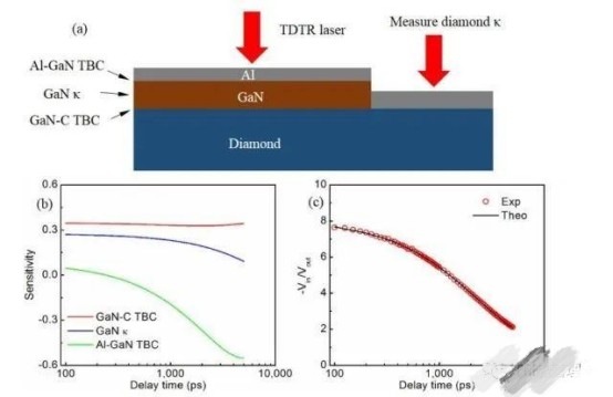
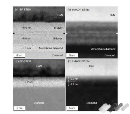
In this study, the experts helped GaN bind to the diamond by adding some silicon atoms at the interface to help the chemical adhesion of the interface and reduce thermal contact conduction. Thermal boundary conduction (or TBC) describes the heat conduction between solid-solid interfaces. The correlation coefficient is a property that indicates the ability to transfer heat across interfaces. The team used two samples. The first sample consisted of a thin layer of GaN (~700 nm) bound to a commercial single crystal diamond substrate (grown by CVD) with a Si sandwich thickness of approximately 10 nm. Another sample combined approximately 1.88 microns thick GaN on a commercial single crystal diamond substrate grown by high-pressure, high-temperature method (HPHT). The thickness of the GaN is polished thin enough for TDTR measurements (Figure 2-4). The thermal conductivity of a single crystalline diamond substrate on a GaN-free region was measured using the following sample structure. A TDTR measurement is then made on the area with a GaN layer to measure the TBC of the GaN-diamond structure. "The measured thermal conductivity of the diamond substrate is used as a known parameter to adjust the TDTR data to extract TBC when measured above the GaN layer. Overall, there are three unknown parameters: Al-GaN TBC, GaN thermal conductivity, and GaN-diamond TBC. TDTR is a technique for measuring the thermal properties of nanostructured materials and bulk materials. One modulated laser beam heats the sample surface, while the other delayed beam detects changes in surface temperature by heat reflection and is captured by a photodetector," the researchers mentioned.
Figure 2: (a) TDTR measurements of diamond and bound GaN-diamond samples. (b) TDTR sensitivity for three unknown parameters. (c) Samp2 TDTR data fitting at room temperature with a modulation frequency of 2.2 MHz

Figure 3: Cross-sectional image of the GaN-diamond interface for (ab) sample 1. (cd) Cross-sectional image of the GaN-diamond interface for sample 2.
CSMH is an enterprise focusing on the research and production of diamond. At present, we offer three solutions combining diamond and GaN: GaN on diamond, Diamond on GaN and diamond wafer(Ra<1nm) required for diamond bonding with GaN, customized products can achieve Ra<0.5nm). And the products are widely used in 5G base stations, lasers, new energy vehicles, new energy photovoltaics and other fields. We always adhere to the concept of providing customers with "high-quality, low-cost, large-area products", and provide customers with the best and most complete diamond thermal management solutions.
 闽ICP备2021005558号-1
Leave A Message