In the past decade, the research boom of gallium nitride (GaN) has swept the global electronics industry. GaN has excellent properties such as large bandgap (3.39eV at room temperature), high breakdown electric field strength (3.3MV/cm), high saturated electron velocity (2.5 × 107cm/s), high thermal conductivity (1.5W · cm-1 · K-1), strong radiation resistance, and easy formation of heterostructures. It is very suitable for the development of high-frequency, high-power microwave, millimeter wave devices and circuits, and has extremely high application value in 5G communication, aerospace, national defense and other fields.
The most basic component suitable for high-power and high-frequency device applications is GaN high electron mobility transistor (HEMT). However, with the continuous improvement of epitaxial material crystal quality and device technology, the reliability and stability of GaN based microwave power devices are seriously challenged under the conditions of miniaturization and power increase.
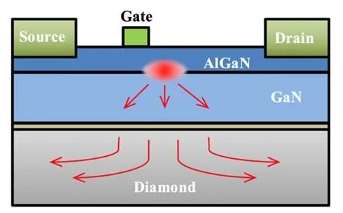
The main reason is that as the power density of GaN based power devices increases, the thermal accumulation effect in the active region of the chip rapidly increases. Local hotspots of tens of nanometers in size are generated near the gate, and the local heat flux density can reach more than ten times the heat flux density on the solar surface. But these heat cannot be quickly and effectively dissipated, which leads to rapid deterioration of its various performance indicators and reduced lifespan. Although the theoretical output power density of GaN power devices can reach over 40 W/mm, the current power density of GaN HEMT devices is only 3-5 W/mm due to their own thermal effects.

Schematic diagram of GaN high electron mobility transistor
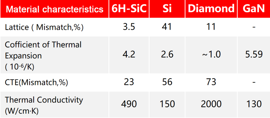
Due to the demand for heat dissipation, the substrate materials for GaN devices have evolved from sapphire (33 W/m · K), Si (thermal conductivity 149 W/m · K), GaN (200 W/m · K) to SiC (thermal conductivity 380 W/m · k) currently on the market. By comparing various substrate materials, we can also see that the thermal conductivity of sapphire substrate is too low (33 W/m · K), while GaN substrate has a higher thermal conductivity (200 W/m · K) but is relatively expensive. Si based GaN devices have average performance but have price advantages. SiC based GaN devices are currently an irreplaceable choice for radar and electronic warfare equipment. Diamond has the highest thermal conductivity among known materials (2000W/m · k), and direct bonding with diamond as a heat dissipation substrate is an ideal choice for reducing thermal resistance.

Performance of Several Common Substrate Materials
GaN on Si : This method has lower yield than the other two, but its advantage is that it can use low-cost, large-sized CMOS silicon wafers and a large number of RF silicon foundries worldwide.
GaN on SiC : This is the "high-end" version of radio frequency gallium nitride. GaN on SiC can provide the highest power level of GaN products and other excellent features to ensure its use in the most demanding environments.
GaN on Diamond : Industrial diamond has the highest thermal conductivity among all materials in the world (therefore it is best used for heat dissipation). Using diamond instead of Si, SiC, or other substrate materials can leverage the high thermal conductivity advantage of diamond and achieve an effective thermal conductivity surface very close to the chip.
Based on mature bonding processes, CSMH has launched GaN-diamond heterojunction integrated composite substrates. Compared with traditional SiC based GaN power devices, diamond based GaN devices have higher heat dissipation capabilities and are expected to achieve miniaturization and high-power of GaN based power devices, thereby promoting widespread applications in the fields of RF power devices and microwave power devices.In addition, the surface roughness of CSMH diamond wafers is Ra<1 nm, which can provide bonding with materials such as Si、GaN、InP、Ga2O3,etc.
 闽ICP备2021005558号-1
Leave A Message