Pos:
Home KnowledgeTechnologyDiamond wafer solves the heat dissipation problem of high-power devicesModern high-power electronic and optoelectronic devices suffer from serious cooling problems due to the generation of a large amount of heat within a small range. As devices become smaller, they still require high reliability in the presence of extreme power densities (greater than 1 kW/cm2). This creates a demand for new thermal management solutions. To cool these devices, it is necessary to place a layer of high thermal conductivity between the device and the cooling system (such as a radiator, fan, or radiator) to propagate narrow heat. Diamond has much better thermal conductivity than copper over a wide temperature range.

Diamond possesses a series of extraordinary properties, including the highest known thermal conductivity, stiffness, and hardness; It has high optical transmission rate, low thermal expansion coefficient, and low density over a wide wavelength range. These characteristics can make diamond the preferred material for thermal management, significantly reducing thermal resistance in various applications. The thermal conductivity of diamond ranges from 1000 (W/m.K to 2200 W/m.K, and diamond also has completely isotropic properties, which can enhance heat propagation in all directions. When using appropriate chip mounting methods, diamond heat sinks can provide reliable solutions for semiconductor packaging with significant thermal management challenges.
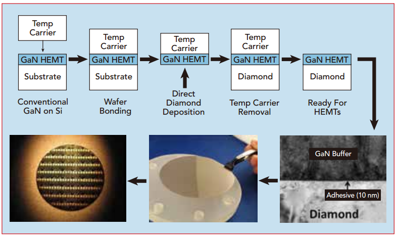
GaN based transistors and their associated radio frequency (RF) power amplifiers (PA) have become the leading solid-state technology to replace traveling wave tubes in radar, electronic warfare (EW) systems, and satellite communications. However, the operation of GaN high electron mobility transistors (HEMTs) on silicon chips presents significant challenges to thermal management, as heat generation is concentrated in very small areas, typically measured in micrometers. The gate spacing in typical GaN HEMT devices is usually less than 50 µ m. This can lead to significant thermal gradients and high operating temperatures, thereby affecting equipment performance and durability. Elevated temperatures can have adverse effects on reliability.

Diamond heat sinks are currently widely used for thermal management in various high-power, high-frequency, high-pressure, high-temperature and other environments. These include components of integrated circuits, heat sinks for high-power laser diodes, and even substrate materials for multi chip modules. The result of these applications in device manufacturing should be higher operating speeds, as devices can be packaged more tightly without overheating. Reliability is also expected to improve, as the junction temperature installed on diamond will be lower for a given device. Research has shown that compared to standard SiC based GaN, using diamond heat sinks can improve RF performance by 20%.

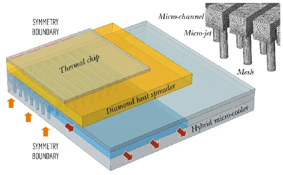
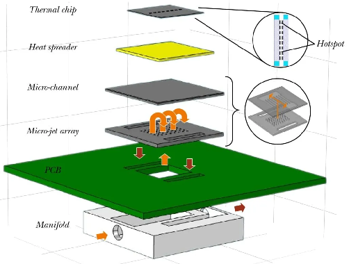
Research has shown that compared to the same SiC based GaN device, the temperature variation of diamond based GaN devices from the GaN channel to the bottom of the substrate is reduced by 80 ℃. By doubling or increasing the thickness of the bonding layer at the diamond cooler interface by four times, no significant temperature increase is expected. For a thermal power of 70W for chip cooling, diamond heat sinks with thermal conductivity coefficients of 2000W/m.K and 1500W/(m.K) can reduce the maximum hot spot temperature by 40% and 38%, respectively. A 2000 W/m.K diamond radiator can emit a heating power of 110W (hot spot heat flux of 10.2kW/cm2) while maintaining the highest hot spot temperature below 160 ℃.

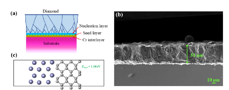
CSMH focuses on the production, research and development, and sales of diamond materials, mastering first-class diamond production processes, and is committed to providing customers with high-power device heat dissipation materials and solutions. Its products include diamond wafers, diamond heat sinks, diamond windows, diamond hetero-integration composite substrates, etc. Among them, the surface roughness of diamond wafer is Ra<1nm, and the thermal conductivity of diamond heat sinks is 1000-2000W/(m · K). Currently, the products have been applied in many fields such as aerospace, power electronics, optical communication, new energy photovoltaics, new energy vehicles, sensors, Al, IGBT, high-speed rail, etc.
 闽ICP备2021005558号-1
Leave A Message