Pos:
Home KnowledgeTechnologyDiamond wafer Bonding and Metallization for Electron Transmission CathodesWe are attempting to fabricate an electron source utilizing the energy in a primary electron beam to generate secondary electrons near one face of a thin diamond sheet and transmit the electrons to the opposite side, where they can be emitted if the diamond surface has negative electron affinity (NEA).[1] We intend to create NEA by exposing the surface to atomic hydrogen. The electron affinity will be lowest when 100% of the surface is hydrogen terminated, but will typically increase with contamination or loss of hydrogen. The probability that an internal electron will be emitted when it encounters the surface is highest when the electron affinity is lowest, and declines as the electron affinity rises even though it may remain negative. To optimize the lifetime and transport properties of the generated electrons, we use single crystal diamond. To promote efficient transmission we plan to apply an electric field throughout the diamond; this requires thin (~10 m) diamond sheets with low trapped charge density and conducting contacts on opposite sides. We grow the diamond in-house on single crystal diamond substrates which have been ion-implanted to facilitate removal of the grown sheet. The thin diamond sheets must be bonded over holes in larger and more robust substrates to allow handling. Since the bonding and fabrication processes are likely to degrade the NEA, we plan to hydrogenate as a final step. The contact and bonding materials should allow operating temperatures as high as possible to allow or facilitate subsequent fabrication steps, bakeout, hydrogenation, and operation.
Potential bonding processes include diffusion bonding, soldering, brazing, and transient liquid phase (TLP) bonding. Diffusion bonding may be the most desirable method for this application; however because the method requires that high pressure be applied to the fragile diamond sheets, we chose not to pursue this route at first.
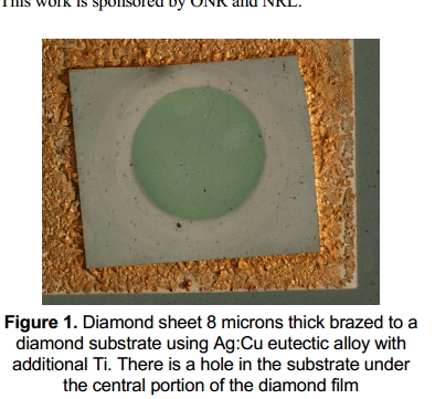
Experiment: We initially bonded the thin diamond sheets over holes in thicker polycrystalline diamond substrates using vacuum brazing and copper-silver eutectic alloy. We applied the appropriate braze thickness (~1 micron) via sputter deposition. Adhesion between diamond and metal requires a chemical bond to form between the metal and diamond. Most transition metals will react with carbon whereas relatively inert metals will not. We ensured wetting by depositing an initial layer of Ti on each diamond surface as well as adding Ti to the braze alloy. A photograph of a diamond film after brazing in vacuum at
800oC is shown in Figure 1. Although the surface of the diamond appears clean by visual inspection, x-ray photoemission spectroscopy (XPS) of the bonded crystal revealed the surface had become contaminated with Ag and Cu. Such contamination prevents the hydrogenation process. More significantly, even if the diamond were cleaned after bonding and activated to NEA, the surface might be degraded by operating at high temperature for many hours.

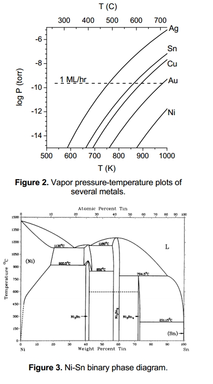
Figure 2 shows a plot of the vapor pressure vs. temperature of several metals. The vapor pressure of Ag at the brazing temperatures (~800oC) is nearly 10-4 torr, or 100 monolayers per second. In most cases only a small fraction of the metal that evaporates will be re-deposited on the diamond, however to ensure that the metal does not evaporate and contaminate the diamond surface, the vapor pressure should be low enough to provide less than 1 monolayer over the relevant time and temperature.
Assuming complete hydrogenation requires heating to 500oC for one hour, any Ag present could cause significant contamination whereas Sn would pose little risk. The TLP method can be used to create a low temperature solder bond with pure Sn, yet allow the joint bond to be reheated to much higher temperatures. This happens when the Sn reacts with another metal. Cu, Au, and Ni are commonly used for this purpose. We have implemented TLP bonding using Au and Ni. The binary phase diagram of the Ni-Sn system is shown in figure 3. To create the TLP bond, we deposit Cr/Pt on both the thick substrate and thin diamond film, then deposit separate layers of Ni and Sn, taking care to provide several moles of Ni for each mole of Sn. We then assemble the joint and heat it to approximately 400oC in vacuum for several minutes. The Sn melts and begins to react with the facing Ni metalforming Ni3Sn4, Ni3Sn2, and Ni3Sn which melt at 800-900oC. Over time all of the Sn reacts with the Ni until noliquid Sn remains. Eventually the Sn compounds will become well dispersed in a matrix of pure Ni.
We prefer using Ni over Au or Cu because the vapor pressure of the reacted Sn will be much lower than pure Sn. The vapor pressure will be reduced by the additional binding energy of the compounds formed, about 24 kJ/mole for Ni3Sn4, and 35 kJ/mole for Ni3Sn2.These energies add to the condensation energy of pure tin (290 kJ/mole), for a total of at least 315 kJ/mole. Dilution in Ni causes additional vapor pressure reduction, so the vapor pressure should be comparable to pure Au (330 kJ/mole), allowing many hours of operation at 500-600oC. We have made several test bonds with polycrystalline diamond, NEA activation and emission tests with a thin diamond film mounted with the Ni-Sn TLP bond are planned.

CSMH has been committed to the research and development and production of diamond materials. Now it has products such as diamond heat sink,diamond wafer, diamond window to provide customers with a comprehensive thermal management solution.
 闽ICP备2021005558号-1
Leave A Message