Pos:
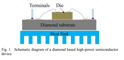
Home KnowledgeTechnologyLow Temperature Bonding Diamond wafer to Si by Using Au Thin-layer for High-power Semiconductor DevicesAs the semiconductor devices are getting higher frequency, higher power and smaller size, the management of thermal dissipation becomes a big challenge. Thermal accumulation increases rapidly in the active region of electronic devices, forming local hotspots and leading to the significant degradation of performance .Therefore, how to manage the heat dissipation becomes one of the key technical bottlenecks restricting the further development of high-power semiconductor devices. Recently, a falling price of artificial polycrystalline diamond was achieved through mass production. The application of diamond as heat dissipation substrate has been placed great expectation due to its ultra,high thermal conductivity, which could reach up to ~2000 W/m·K . Fig.1 shows the schematic diagram of a diamond based high-power semiconductor device.
Although diamond can be directly grown on the semiconductor wafers by chemical vapor deposition (CVD), the growth of diamond needs an environment of more than 700℃, which is unacceptable for semiconductor devices to withstand such high temperature. Surface Activated Bonding (SAB) technology can bond a single-crystal diamond to device at room temperature by using Ar beams for activation. But it needs extremely smooth surface, which is very challenging for polycrystalline diamond. Another method is soldering diamond to semiconductor devices .

However, the thermal conductivity of solder layer is typically two orders of magnitude smaller than that of diamond, and the bonding requires thick filler of metal layers. That introduces huge thermal resistance and thus significantly degrades the heat dissipation performance of diamond.
In this study, novel Au thin layer was used for the low temperature bonding of polycrystalline diamond and Si. The Au-Au atomic diffusion bonding was successfully achieved. Scanning acoustic microscope (SAM) was used to determine the bonding porosity. The effects of surface roughness and flatness on the porosity were discussed. The technological route of diamond heat dissipation substrate for high-power semiconductor devices needs more optimization.
Au thin layer was used for the low temperature bonding of polycrystalline diamond and Si. The Au-Au atomic diffusion bonding was successfully achieved. Clean processes were optimized. SAM was used to determine the bonding porosity, which typically exceeded 10%. AFM tests show that the typical diamond surface roughness was Ra>1nm. In addition, the poor surface flatness (TTV≥2μm) of diamond contributed to the degradation of bond-ability. The effect of surface roughness on solid-state diffusion bonding was discussed. Future work needs to flatten the diamond surface and study the influence of diamond thickness and thermal conductivity on the heat accumulation effect of semiconductor devices. Develop and optimize the technological route of diamond heat sink for high-power semiconductor devices.
CSMH has been committed to the research and development and production of diamond materials. Now it has products such as diamond heat sink sheet,diamond wafer, diamond window to provide customers with a comprehensive thermal management solution.
 闽ICP备2021005558号-1
Leave A Message