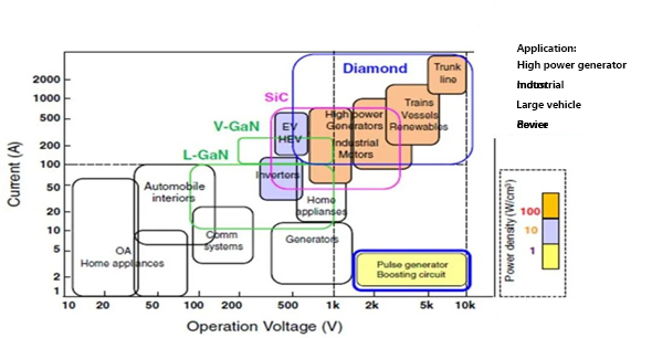
Diamond material has the characteristics of high carrier mobility, high carrier saturation drift rate and strong breakdown field. It is an ideal material for manufacturing high power, high temperature and high frequency devices. Due to its band gap width, high thermal conductivity, breakdown electric field strength and extremely high charge mobility (electron mobility of CVD diamond >3000cm2/V.s), diamond diamond has the advantages of high charge mobility. Diamond semiconductor devices can operate in very harsh environments such as high frequency, high power, high voltage and strong radiation, which is known as the "ultimate semiconductor material".
In addition, diamond has high spectral transmission performance in a wide wavelength range from ultraviolet to far infrared, and is the optical window material for high-power infrared lasers and detectors. At the same time, it has acid resistance, alkali resistance, resistance to various corrosion gas erosion performance, is an excellent corrosion resistant material.
-- Material properties --
1. Extremely high dielectric breakdown characteristics: The breakdown voltage is 107V, which is 50 times of gallium arsenide material, 2 times of gallium nitride material and 2.5 times of silicon carbide material.
2. Extremely high power capacity: the allowable power usage capacity of diamond is more than 2500 times that of silicon material; Especially suitable for making high power electronic devices.
3. Extremely high heat conduction: Diamond has the highest thermal conductivity at room temperature, 5 times that of copper.
4. Low dielectric constant: The dielectric constant of diamond is 5.7, which is about half of gallium arsenide and less than half of InP. In other words, diamond semiconductor has a competitive capacitive load at a given frequency, which provides great convenience for the design of millimeter wave devices.
5. High saturated carrier velocity: the saturated carrier velocity of diamond is 12.7 times that of gallium arsenide, silicon or indium phosphide, and the carrier velocity is larger than the peak value of gallium arsenide, that is, it can maintain its high rate even when the electric field intensity increases.
-- Application field --
As a kind of wide-band gap semiconductor material, diamond integrates mechanical, electrical, thermal, acoustic, optical, corrosion resistance and other excellent properties, which is one of the most promising third generation semiconductor materials. It has great application potential in many fields such as high temperature and high power power power devices, microwave power devices, deep ultraviolet light and high-energy particle detectors, deep ultraviolet light emitting devices, single photon light sources, biological and chemical sensors, micro-electromechanical (MEMS) and nanoelectromechanical (NEMS) devices, and spintronics.
High power power electronics
The band gap of diamond semiconductor material is up to 5.47 eV, and the thermal conductivity is the highest among known semiconductor materials. Therefore, diamond semiconductor material can meet the requirements of high power, strong electric field and radiation resistance in the future, and is an ideal material for making power semiconductor devices.

Deep ultraviolet detector, high-energy particle detector
In the field of deep ultraviolet optoelectronics, diamond has inherent advantages in deep ultraviolet detectors and high-energy particle detectors under extreme conditions due to its large band gap, high temperature and radiation resistance. It is also based on the above reasons and can avoid the unsolved diamond doping problem in the process. Therefore, diamond detector is the only product type related to semiconductor diamond devices that is relatively mature and has been productized at present.
Substrate material
Diamond can also be used as a substrate for GaN power devices to help dissipate heat for higher frequencies and higher power. Starting in 2008, the European Union invested in promoting the chemical vapor deposition (CVD) method to grow diamond on the back of GaN devices. And then the Defense Advanced Research Projects Agency, the Office of Naval Research and others poured in a lot of money United Universities (University of Bristol, Georgia Tech, Stanford, etc.), semiconductor companies (Element Six, Raytheon, Qorvo, Lockheed Martin, Northrop Grumman, etc.) vigorously promote the development of diamond-based GaN devices. However, due to the high price, the application of gallium nitride devices on diamond substrates is limited to the fields of national defense and aerospace.
 闽ICP备2021005558号-1
Leave A Message