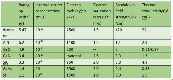
Diamond is an ultra-wide bandgap semiconductor material with a band gap of 5.5 eV, which is larger than wide bandgap semiconductor materials such as GaN and SiC. As shown in the table below, the diamond band gap is 5 times that of Si; The carrier mobility is also 3 times that of Si materials, and theoretically the carrier mobility of diamond is more than 2 times higher than that of existing wide bandgap semiconductor materials (GaN, SiC), and diamond has a very low intrinsic carrier concentration at room temperature. And, in addition to the highest hardness, diamond has the highest thermal conductivity of any semiconductor material, 7.5 times that of AlN. Based on multiple excellent performance parameters such as high voltage resistance, large radio frequency, low cost, and high temperature resistance, diamond is considered to be the most promising material for the preparation of the next generation of high-power, high-frequency, high-temperature and low-power loss electronic devices, and is known as the "ultimate semiconductor" in the industry.

Figure 1 Comparison of the characteristics of several semiconductors
It is precisely because of the performance of diamond, from materials to devices, the research and development of diamond in recent years has made remarkable progress. For a long time, people began to develop and study diamond. In the 70s of the 20th century, American scientists developed the use of high temperature and high pressure method (HPHT) to grow small blocks of diamond single crystals, which opened the boom in diamond research. In recent years, with the advent of the post-Moore era, people's R&D investment in the field of new materials has been increasing, and the development of ultra-wide bandgap semiconductor materials such as diamond has also accelerated. There are major new technological breakthroughs in both material preparation and devices.
In terms of materials and preparation:
The preparation methods of diamond are mainly divided into high temperature and high pressure method (HPHT) and plasma chemical vapor deposition method (PCVD).
High Temperature High Pressure (HPHT) belongs to thermodynamic equilibrium growth. According to the carbon phase diagram, it can be seen that the stable phase under high pressure is diamond, which converts graphite into diamond by using external pressure and temperature. The source of carbon in the growth process is usually graphite, through the catalyst hydraulic device, under the catalytic action of the metal melt, maintain a constant ultra-high temperature, high pressure conditions (usually pressure of about 5.4 GPa, temperature of about 1400 °C), the carbon source is transported by the metal catalyst to the seed surface in the low temperature zone and continuously deposited into lab-grown diamonds.
Chemical vapor deposition (CVD) uses chemical reactions of gas precursors under specific conditions and substrates to form the required thin film material. In the preparation of single-crystal diamond materials, methane and hydrogen are usually used as precursors, and single-crystal diamond is used as the substrate under low-pressure conditions of high temperature (about 1000 °C) and semi-vacuum, and is grown in a gas phase epitaxy manner. Since the stable phase of carbon under atmospheric pressure is graphite phase, a steady stream of plasma hydrogen atoms is required to surround methane (CH4) and decomposition products surrounding the sp3 structure in the process of growing diamond by CVD method, and promote the attachment of activated carbon atoms to diamond seed crystals by controlling the sedimentary growth conditions.
In general, compared with HPHT method and other PCVD methods, MPCVD has stepless discharge, no pollution, strong epitaxy controllability, and has obvious advantages in the preparation and doping of large-size and high-purity diamond, and is the preferred method for the preparation of high-quality and multi-field application of diamond. In addition, compared with polycrystalline diamond, single crystal diamond (SCD) without grain boundary constraint has better optical and electrical properties, and has outstanding application effects in cutting-edge scientific and technological fields such as quantum communication/computational radiation detectors, cold cathode field emission displays, semiconductor lasers, supercomputer CPU chips, multi-dimensional integrated circuits and military high-power radar microwave traveling wave tube thermal conductive support rods, and the preparation of large-size and high-quality SCDs is the premise. Diamond, as a wafer, must be more than 2 inches in size. At present, the technologies for preparing large-size diamonds and wafers mainly include homogeneous epitaxial growth, mosaic wafer preparation and heteroepitaxy growth. Among them, the independent single crystal sheet grown by homogeneous epitaxy has the characteristics of low defect density, and the maximum size can reach 1 inch; Wafers with diamond heteroepitaxy can reach up to 4 inches. If it is a low-cost heteroepitaxy CVD method, the development and application of diamond polycrystalline films have been very active, and the wafer has reached 8 inches, which can be used as a thermally conductive substrate for a new generation of GaN power electronic devices. Therefore, the research of diamond materials is required to develop in the direction of large size, low defect, low resistivity and high thermal conductivity.
In the research of diamond devices:
1. Diamond doping problem
For diamond semiconductor devices, doping of diamond materials is the basic technology for the formation of power devices, and has always been a research hotspot. The biggest problem with the commercialization of diamond semiconductors is that the efficient bulk doping of diamond has not been solved, and it is easy to manufacture P-type transistors and difficult to manufacture N-type transistors. Due to the dense structure of diamond with small gaps. Traditional elemental doping techniques usually cause severe lattice distortion of diamond, and lead to deep energy level doping, and room temperature carrier activation is difficult.
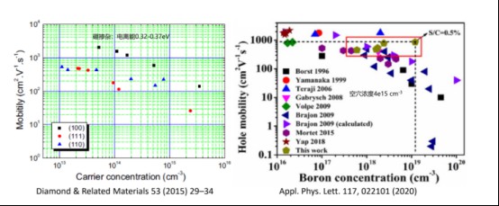
At present, the p-type doping technology of diamond is relatively mature, and the main doping substance is boron atom. For p-type diamonds, boron impurities can easily be incorporated into natural diamonds and MPCVD diamonds without crystal orientation problems, but the activation efficiency of boron at room temperature is less than 0.1%. The doping concentration and mobility of boron in diamond is a trade-off relationship, excessive doping concentration often leads to a rapid decrease in mobility, when the boron doping concentration is 1019 cm-3, the mobility will be reduced to 100 cm2· V-1·s-1 or below. The position of the diamond's C atom ( covalent radius 0.077 nm ) in the periodic table , with the nearest being the nitrogen ( N ) atom ( 0.075 nm ) , making it also a favorable candidate for n-type doping of diamond. However, due to the accompanying Jahn-Teller effect, the N atoms of the C atoms in the displacement diamond after doping are skewed in the local lattice, and the N atoms deviate from the position of the displacement, and its doping energy level is very deep, 1.7 eV, which is difficult to produce conduction at room temperature.

Fig. 2 Ionization energy and hole concentration of boron doped with diamond
2. Progress in the application of diamond devices
The era of 5G communication is rapidly and comprehensively unfolding, and the application of diamond single crystal materials in semiconductors and high-frequency power devices is becoming increasingly prominent. Diamond single crystal and products are an important material basis for the implementation of major national strategies such as ultra-precision machining and smart grid, and the upgrading of industrial clusters such as intelligent manufacturing and 5G communication, and the breakthrough and industrialization of related technologies are of great significance to the independent security of intelligent manufacturing and big data industries.
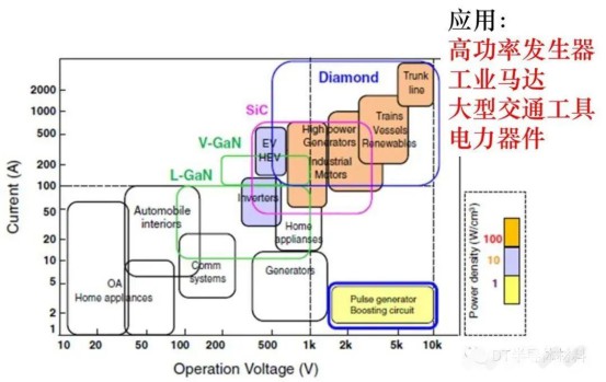
Diamond can be used as an active device material to make FETs, power switches and other devices, and can also be used as a passive device material to make Schottky diodes. Because diamond has high thermal conductivity and extremely high charge mobility, the semiconductor devices made of diamond can be used in harsh environments such as high frequency, high power and high voltage, and have great application prospects.

Figure 3 Schematic diagram of diamond semiconductor application field
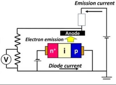
(1) One area where diamond is superior to other materials such as SiC is its high dielectric breakdown strength and high critical electric field. This advantage may benefit from reducing the on-resistance of Schottky barrier diode (SBD) breakdown voltage capability in high-power engineering equipment and applications.

Figure 4 An example of vacuum power switching using a diamond PiN diode in the transmit current
(2) In the field of power electronics, it is developing in the direction of high breakdown voltage, high breakdown field strength, high temperature operation, low on-resistance, high switching rate and normally off devices. Diamond transistors are mainly used in various FETs, including metal semiconductor field effect transistors (MESFETs), MOSFETs and JFETs, and there are two kinds of channels: two-dimensional hole gas and p-type doped layer on the surface of diamond hydrogen terminal. With the advancement of n-type doped materials, bipolar diamond devices have begun to appear, and heterojunction bipolar transistors have recently been developed. In the field of microwave electronics, hydrogen terminal FET is the mainstay, and it is developing in the direction of high fT/fmax and high power density.

Figure 5 Schematic diagram of diamond MEMS chip and diamond cantilever integrated into the chip
CSMH is an enterprise focusing on the research and production of diamonds, the core products are diamond wafers, diamond heat sinks, diamond-based gallium nitride epitaxial wafers and aluminum nitride films, etc., and the product quality has reached the world's leading level. The thermal conductivity of diamond heat sink sheet reaches 1000-2000W/m.k, and the surface roughness of diamond wafer growth surface is Ra < 1 nm. Products are widely used in 5G base stations, lasers, new energy vehicles, new energy photovoltaic and other fields. High-power semiconductor devices using diamond heat sink have been used in optical communications, and are also used in RF power amplifiers, laser diodes, power transistors, electronic packaging materials and other fields. We will always adhere to the concept of customer first, and continue to provide customers with the best products and services.
 闽ICP备2021005558号-1
Leave A Message