Pos:
Home KnowledgeTechnologyRoom-temperature bonding of Mo/Au nanolayers to GaN on diamond wafers for high-power devicesGaN semiconductor material has great technical potential in the applications of power electronic devices due to its high electron saturation velocity and high breakdown voltage. However, to date, GaN devices are mainly fabricated on sapphire, Si and SiC substrates having the thermal conductivities of about 0.5, 1.5 and 4.0W/cm·K, respectively, which make the heat accumulated at the hot spots of AlGaN/GaN heterojunctions not removed effectively. Heat dissipation is a bottleneck problem restricting the application of GaN devices in high-power semiconductor devices at present. In order to solve the problem, a lot of researchers focus their attention on GaN-on-diamond structure, by which the heat generated in GaN devices can be easily dissipated due to the excellent thermal conductivity characteristics of diamond (thermal conductivity: ~22W/cm·K), and thereby output power and reliability of GaN devices can be significantly improved.

Fig. 1. Schematic illustration of the bonding process of GaN/diamond wafers performed at room temperature by using Mo/Au nano-layer.
Recently, room temperature bonding techniques have been reported. One is the room temperature direct bonding, which has been developed for bonding of semiconductor wafers such as Si/GaAs, p-Si/n-GaAs, GaAs/SiC, p-Si/n-InP, SiC/SiC and Diamond/Si. The bonding of wafers with nano-films coated on their surfaces is another method to achieve wafer bonding at room temperature. F. Mu et al. realized the bonding of GaN on diamond through Si-based nano-adhesion layer at room temperature by surface-activated-bonding (SAB) method for the first time.

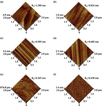
Fig. 2. AFM images of (a) an original polycrystalline diamond wafer, (b) an Mo/Au film deposited on polycrystalline diamond wafer, (c) an original single-crystalline diamond wafer, (d) an Mo/Au film deposited on single-crystalline diamond wafer, (e) an original GaN wafer and (f) an Mo/Au film deposited on GaN wafer.
Fig. 2 shows the AFM images of original polycrystalline diamond wafer, single-crystalline diamond wafer, GaN wafer, and Mo/Au films deposited on these three wafers, whose the root-mean-square (RMS) surface roughnesses were 1.300nm, 0.824nm, 0.509nm, 0.685nm, 0.265nm and 0.438nm, respectively. It can be seen from Fig. 2(a)–(b) that the surface roughness of Mo/Au film deposited on polycrystalline diamond wafer was obviously lower than that of original polycrystalline diamond wafer. This may be due to the existence of striped protrusions and depressions on the surface of original polycrystalline diamond wafer, and the deposited Mo/Au film can fill these depressions and make the diamond surface smoother, so the surface roughness of deposited Mo/Au film decreases. The surface roughnesses of Mo/Au films deposited on single-crystalline diamond and GaN wafers were slightly higher than that of the original single-crystalline diamond and GaN wafers as shown in Fig. 2(c)–(f). This may be due to the fact that original single-crystalline diamond and GaN wafers are extremely smooth, while the deposited Mo/Au films consist of nano-grains, which leads to the increase of surface roughness. The results show that the Mo/Au films deposited on these three wafers remained an atomically smooth surface which is beneficial to high-quality wafer bonding.

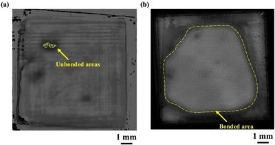
Fig. 3. SAM images of the sample II (a) before and (b) after 1000-cycles thermal cycling testing.
Due to the self-heating effects, GaN-based devices will be subjected thermal impact during operation. In order to evaluate the thermal-impact-resistance performance, the sample II was carried out thermal cycling testing which was kept at minus 45°C for 15min, then heated to 125°C for 15min, and then cooled to minus 45°C for 1000-cycles. The SAM image of the sample II after 1000-cycles thermal cycling testing shown in Fig. 3(b), the GaN wafer was still bonded on the single-crystalline diamond wafer and the bonding area remained 73%, which may be due to the strong adhesion on the Au/Au bonding surface, while the internal stress caused by the different coefficients of thermal expansion between the GaN, diamond and Mo/Au nano-layer multilayer structure was not enough to exceed the adhesion of the Au/Au bonding surface. This result shows that Mo/Au nano-layer can balance the difference of coefficients of thermal expansion between GaN and diamond wafers.
In summary, GaN wafers were bonded on polycrystalline and single-crystalline diamond wafers by using Mo/Au nano-layer at room temperature. A low voidage of 1.5% can be obtained for Mo/Au nano-layer, and the bonding strength is 6.8MPa. After 1000-cycles thermal cycling testing, the bonding area still remained 73%, which indicates that Mo/Au nano-layer can balance the difference of coefficients of thermal expansion between GaN and diamond wafers. This work is expected to be helpful for the applications of diamond-based high-power GaN semiconductor devices.
At present, the diamond and gallium nitride bonding process continues to improve. It has been confirmed by relevant research institutions that the surface roughness of the wafer will affect the bonding yield. For successful bonding, the surface roughness value Ra must be less than 1 nm, ideally less than half of this value, i.e. Ra < 0.5 nm. CSMH uses the MPCVD method to prepare high-quality diamond heat sinks, and uniquely develops a high-efficiency and precision machining method for the atomic-level surface of diamond wafer based on plasma-assisted grinding and polishing. For a 2-inch diamond wafer, the surface roughness can be reduced from tens of microns to below 1 nm. This technique has high removal efficiency and is able to obtain atomically flat surfaces without subsurface damage. For the diamond wafer required for bonding, we provide customized products, and the surface roughness Ra can reach less than 0.5nm.
 闽ICP备2021005558号-1
Leave A Message