Pos:
Home KnowledgeTechnologyMore than you can imagine, about the "photothermal electricity" of diamond wafer!Have you ever imagined that there is a semiconductor material that not only excels in heat and electricity, but also in optics? You must be very curious about what it is, today let's take a brief analysis of the "light and heat" of diamond.
The “heat”of diamond
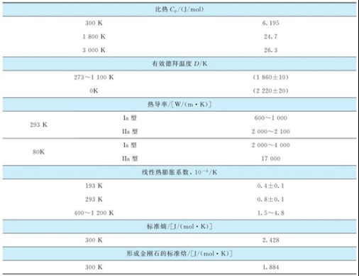
The thermal conductivity of pure impurities-free diamond is extremely high. It is the solid material with the highest known thermal conductivity at room temperature, with a thermal conductivity of about 5 times that of copper metallic. Metal heat transfer is achieved by electron transport, and the diamond heat transfer mechanism is different from the metal heat transfer mechanism, which transfers heat through lattice vibration, characterized by phonon flow, equal to the lattice vibration frequency multiplied by Planck's constant. Carbon atoms are very small, atomic mass is also very small, the carbon atoms in the diamond structure are closely bound to each other isotropically, and the result is that the quantum energy of the vibration of carbon atoms is large, that is, the vibration frequency is very high, the maximum value is 40×1012Hz, therefore, the thermal conductivity is very high. Its ultra-high thermal conductivity is expected to achieve near-perfect heat dissipation in the field of high power, as a heat sinking material, diamond can be deposited in the GaN channel at a size of hundreds of nanometers, so that transistor equipment can effectively dissipate heat when operating.
Thermal expansion in crystalline materials refers to the phenomenon that when the atom obtains energy when increasing the temperature, the amplitude of the lattice vibration increases and the atomic spacing increases. Since diamond is a covalently bonded crystalline material, it has a relatively small coefficient of thermal expansion, the coefficient of thermal expansion (CTE) at room temperature is 0.8×10⁻⁶/°C, the coefficient of thermal expansion of copper is 17×10-6/°C, and the coefficient of thermal expansion of graphite within the surface (ab axis) is slightly negative. Unlike graphite, which is anisotropic in thermal expansion, the coefficient of thermal expansion of diamond is isotropic and gradually increases with increasing temperature. The specific heat of diamond is comparable to that of graphite, but higher than that of many metals, and as with all other elements, the specific heat of diamond increases with increasing temperature.

Figure 1 Thermal properties of diamond
The “light”of diamond
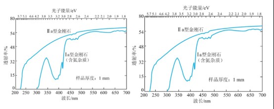
The characteristics of electromagnetic radiation through the material can be characterized by transmittance, defined as the ratio of the radiated power of the permeable material to the incident power, and the wide spectrum transmittance is one of the excellent optical properties of diamond. The high transmittance of diamond is related to its wide band free nature and the strength of covalent bonds. In fact, diamond is the widest electromagnetic band-through material, and its light transmittance covers X-rays to microwave and millimeter wave bands.

Figure 2 a (left) and b (right) show the transmission spectrum of the UV-visible region and the infrared light region of diamond, respectively
Pure diamond material has only two intrinsic absorption bands: an ultraviolet absorption band located in the short wavelength spectral region, with an absorption side of 230 nm, which corresponds to the inter-band transition of electrons; The other is an absorption band located in infrared 1400~2350cm-1, which is related to phonons. The infrared region with a wavelength longer than 7 mm has zero absorption and also includes an atmospheric window of 8 to 14 mm. It can be seen that pure and defect-free diamond materials are ideal optical materials, but the actual diamond material has more or less impurities and lattice defects inside, which will produce additional absorption bands, which are located in the infrared absorption region.
The most typical luminescence characteristic of diamond is visible fluorescence, mainly in the blue and green light regions, and these fluorescences come from electromagnetic radiation produced by the transition of electron states in the band gap, which are formed by impurities and lattice defects. In addition, the cathode fluorescence of diamond is called A-band fluorescence, and the spectral peak is located at 2.4 to 2.8 eV, corresponding to green light and blue-violet light.

Figure 3 Optical properties of diamond
Diamond's “electricity”
Diamond has excellent semiconductor characteristics and is one of the most promising broadband semiconductor materials, it has an indirect band gap and a band gap width of 5.47 eV. When heating, due to thermal excitation, the probability of electrons in semiconductors jumping from valence band to conduction band increases, and the conductivity of semiconductors also increases. The wider the band gap, the smaller the probability of electron transition, which is why wide bandgap semiconductors are used at high temperatures.
By the appropriate amount of doping can be transformed from an intrinsic semiconductor at room temperature to a non-intrinsic semiconductor, such as boron (B), p-type diamond semiconductors can be obtained, phosphorus doped (P) can obtain n-type semiconductors, doping can be achieved in high-pressure or CVD growth diamond, natural IIb type diamond is doped semiconductor, but it is rare in nature, diamond also has a high electron mobility and high saturated electron mobility. At present, the room temperature electron and hole mobility of diamond thermal sedimentation films prepared by plasma CVD on diamond substrate has reached 4500cm2/(V·s) and 3800cm2/(V·s), respectively.

Figure 4 Electrical properties of diamond
CSMH is a high-tech enterprise focusing on the research and development and production of third-generation (wide bandgap band) semiconductor substrate materials and devices, and is committed to becoming the world's leading wide bandgap semiconductor materials and devices company. We have always adhered to the concept of customer first, to provide customers with the best products and services. At present, the company has realized the large-scale production of diamond and aluminum nitride related products, the existing diamond wafer Ra<1nm, diamond thermal imposition sheet thermal conductivity 1000-2000W/m.k, and GaN on diamond, Diamond on GaN, diamond-based aluminum nitride and other products. And has been widely used in 5G base stations, lasers, new energy vehicles, new energy photovoltaics and other fields.Here, we will provide you with the most comprehensive diamond thermal management program.
 闽ICP备2021005558号-1
Leave A Message