CSMH successfully has acheived high-quality AlN (AlN) thin films on silicon substrates, XRD (0002) rocking curve < 0.8°, and surface roughness Ra < 1.5 nm on the growth surface, high-quality AlN films help GaN for large size, high quality and low cost.
Submit requirements and contact us
FWHM @
XRD (0002) <0.9°
Growth Surface Roughness
Ra<1.5nm(200nm)
Facilitating GaN Growth
Facilitating large-scale, high-quality epitaxial growth of GaN
For RF Devices
Effective RF Loss Reduction
CSMH successfully has acheived high-quality AlN (AlN) thin films on silicon substrates, XRD (0002) rocking curve < 0.8°, and surface roughness Ra < 1.5 nm on the growth surface, high-quality AlN films help GaN for large size, high quality and low cost.
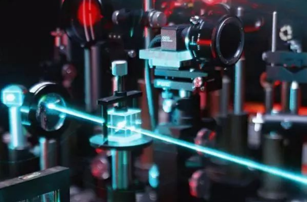
Aluminum nitride (AlN) is an ultra-wide bandgap semiconductor material with many excellent properties, such as the 6.2eV band gap, high breakdown field strength, high saturation electron mobility, high chemical and thermal stability. Therefore, AlN is particularly useful as a substrate material for the deep ultraviolet (DUV) LEDs, and other high-power, high-frequency electronic devices. Nowadays, AlN is the preferred piezoelectric material for GHz-level surface acoustic wave (SAW) devices due to its excellent thermal stability, chemical resistance, and low propagation losses.
Advantages of AlN
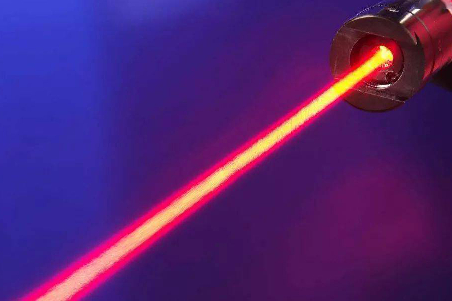
• Wide bandgap of 6.2eV, it is an important material for the DUV LEDs (UVC band, 200 – 300 nm)
• Material properties that are ideal for high-temperature, high-frequency, and high-power devices: 1) high breakdown electric field, 2) high thermal conductivity, 3) high electric insulation, 4) low dielectric constant, 5) low coefficient of thermal expansion, 6) good mechanical properties, 7) and corrosion resistance.
• Best materials for the sensors, actuators and filters with very good piezoelectric properties (especially along the C-axis)
• A preferred substrate material for heteroepitaxial growth of gallium nitride (GaN)-based optoelectronic devices due to its very close lattice constant and thermal expansion coefficient to GaN crystal
Excellent Physical Properties of AlN
•Atoms are bound by covalent bonds, with good chemical stability and high melting point;
•It is a piezoelectric and dielectric material with high mechanical strength and electrical insulation.
•The crystal film has high hardness and can be used as wear-resistant coating;
•High resistivity, low leakage current and high breakdown field strength make it one of the best choices for insulating buried layer materials in microelectronic devices;
•The fabrication process is compatible with CMOS, and can be integrated with other devices on the same chip;
• It is a wide and direct band gap optoelectronic material capable of emitting blue and ultraviolet light with high efficiency;
•It has outstanding piezoelectricity and high-speed propagation performance of surface acoustic wave along the c-axis, and its the sound transmission speed is the highest of all inorganic nonferrous piezoelectric materials.
Applications of AlN
AlN films with unique and excellent material properties have numerous applications in a variety of fields, such as optoelectronic, piezoelectric devices, heteroepitaxy, silicon on insulator (SOI), and packaging.
1)Energy efficient AlN-based LED provides the blue light and ultraviolet light.
2)AlN-based GHz-level SAW device with a large electromechanical coupling constant and low dispersion at high frequency, resulting in the highest SAW velocity.
3)AlN film is also an excellent transition layer used for GaN epitaxial growth on silicon carbide (SiC) and sapphire substrates.
4)Insulating buried layer of SOI material instead of SiO2.
5)Isolation medium and insulating material in the packaging of electronic devices and integrated circuits.
AlN on Si-001
Substrate) : 500±10μm Si(111), Customized
Inch: 2、4……Customized
AlN Thickness : 5~200nm, Customized
Orientation: c-aixs [0001]
Ra (nm) (5x5μm): Ra< 1.5nm (200nm)
HRXRD FWHM@ (0002) : <0.8°
Warp: <30μm
Bow: -10 ~15μm
Packaging: Single/Multi Wafer Cassette
application area
MORE 闽ICP备2021005558号-1
Leave A Message