Pos:
Home KnowledgeTechnologyDiamond on GaN HEMT, a new idea to solve the heat dissipation of gallium nitride (GaN)!At present, gallium nitride (GaN) is mainly used in the fields of radio frequency and fast charging, and its heat dissipation problem has caused extensive research at home and abroad. The combination of GaN/diamond can greatly improve the heat dissipation efficiency of the device, increase the heat transfer capacity and output power density inside the chip, improve the high-power characteristics and reliability of the device, and break down the main obstacles that hinder the potential of gallium nitride GaN devices. .
In order to obtain a diamond-based GaN HEMT device with higher effective thermal conductivity, currently three methods are mainly used to achieve the combination of a diamond substrate and a GaN epitaxial material. Including direct epitaxial growth of GaN structure on diamond substrate, growth of diamond on GaN HEMT structure, GaN/diamond bonding. Not long ago, the editor has introduced the GaN/diamond bonding method. Today, I will introduce another method, which is to use the chemical vapor deposition (CVD) method to directly grow diamond on the GaN HEMT. This method generally uses a growth temperature higher than 600°C, and can choose to add a seed layer such as aluminum nitride or silicon nitride between the GaN layer and the diamond. At present, the optimal RF performance of the device obtained by this method is that the output power density under the bias voltage of 10GHz and 40V reaches 7.9W·mm-1, and the PAE reaches 46% [1].
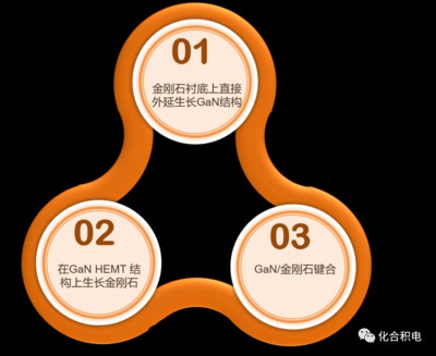
Three methods of combining diamond substrate and GaN epitaxial material
The technical difficulty of growing diamond on GaN HEMT structure lies in the problem of lattice mismatch and large thermal mismatch between diamond and gallium nitride, and the high temperature and strong plasma required for diamond growth can easily damage the gallium nitride surface. This makes it difficult to grow diamond on the GaN HEMT structure. we continues to conquer core technologies and has successfully solved these technical difficulties in the near future.
At present, we uses microwave plasma chemical vapor deposition equipment to achieve epitaxial growth of polycrystalline diamond material with a thickness of<10um on 50.8 mm (2 inches) silicon-based gallium nitride (GaN). The transmission electron microscope and X-ray diffractometer were used to characterize the surface morphology, crystalline quality and grain orientation of the diamond film. The results showed that the surface morphology of the sample was relatively uniform, and the diamond grains basically showed a (111) plane growth. Higher crystal plane orientation. During the growth process, the gallium nitride (GaN) is effectively prevented from being etched by the hydrogen plasma, so that the characteristics of the gallium nitride before and after the diamond coating do not change significantly.
Characterize test results
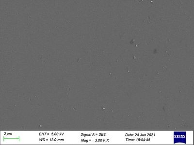
Fig. 1 SEM surface topography of undamaged GaN layer under hydrogen plasma environment (3000 times)
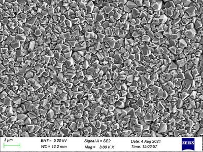
Figure 2 SEM surface topography of diamond nucleation surface grown on GaN (3000 times)
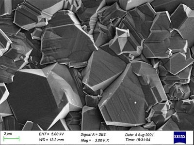
Figure 3 SEM surface topography of diamond surface grown on GaN (3000 times)
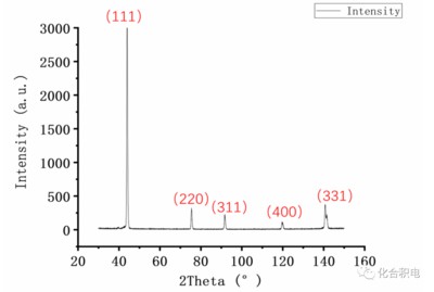
Figure 4 XRD diffraction pattern of diamond film grown on GaN
We leads technological innovation and continuously promotes the maturity and application development of GaN on diamond technology. We will help you achieve major breakthroughs in the core technology of gallium nitride and GaN, and seize market opportunities in solving the heat dissipation of high-frequency and high-power GaN HEMTs. Welcome to negotiate and cooperate!
references:
[1] DUMKA D C,CHOU T M,FAILI F,et al. AlGaN /GaN HEMTs ondiamond substrate with over 7 W /mm output power density at 10 GHz [J]. Electronics Letters,2013,49 ( 20) :1298-1299.
 闽ICP备2021005558号-1
Leave A Message