GaN is one of the third generation of wide bandgap semiconductor core material, it has unique physical advantages, such as wide band gap, strong atomic bonds, high thermal conductivity, chemical stability, strong ability to resist radiation characteristics, very suitable for the preparation of high temperature and high frequency high power devices, usually used in microwave radio frequency, power electronics and optoelectronics three areas. Specifically, microwave rf direction includes 5G communications, radar early warning, satellite communications and other applications; The direction of power electronics includes smart grid, high-speed rail transit, new energy vehicles, consumer electronics and other applications; Optoelectronic direction includes LED, laser, photodetector and other applications.
As a high-power device in various major development fields, the power, frequency, efficiency and reliability of GaN power devices are also put forward higher requirements. It is found that heat dissipation has become a stumbling block in the development of GaN HEMT devices with higher power and efficiency.
The manufacturing process of GaN devices in the market is divided into GaN on SiC, GaN on Si and GaN on Diamond The thermal conductivity of commonly used substrate materials such as silicon and silicon carbide is low, which greatly limits the requirements of heat dissipation and high power performance of devices. Using diamond with high thermal conductivity can improve the heat dissipation ability of GaN devices and further improve the device performance. Diamond has the highest thermal conductivity among the known natural materials. Its thermal conductivity is as high as 2200 W/m·K, which is more than 4 times that of SiC material and 13 times that of Si material. Diamond substrates with high thermal conductivity are ideal for reducing thermal resistance.
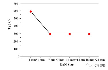
At present, experiments show that GaN RF power devices on different substrates: Si based GaN, SiC based GaN, metal based GaN, and Diamond based GaN RF power amplifier, through the three-layer structure (Gan-diamond-heat sink), changing the Diamond plane size to increase, can effectively improve the heat dissipation effect.

The sensitivity curve of gan-diamond-CuW junction temperature with the size of Diamond
Diamond substrate can not only effectively solve the problem of heat dissipation which is troubled to improve the performance of GaN power devices, but also can be used to manufacture gan-based power devices with higher power density under the same size. When used in phased array chip, the reliability of the system can be significantly improved and the size and cost of the system can be reduced. When used in solid-state power amplifiers, the device size, cost and quality can be significantly reduced and the efficiency can be improved. When used for broadband communication, it can reduce the cost of chip size and improve reliability.
In order to obtain diamond-based GaN HEMT devices with high thermal conductivity, the combination of diamond substrates and GaN epitaxial materials is mainly realized in three ways.
The first is to grow GaN structures directly epitaxy on diamond substrates.
The second is to grow diamond on GaN HEMT structure.
The third is GaN/ diamond bonding method based on transfer technology.
The GaN/ diamond bonding method is more flexible. As a parallel process, GaN epitaxy layer and diamond substrate can be prepared simultaneously before bonding, and then the prepared GaN HEMT can be detached from the original substrate and transferred to the diamond substrate.
Bonding technology is an important technology in the manufacturing process of semiconductor industry, most of the electronic materials, electronic device structure and other connections will be applied to bonding technology. It is a semiconductor manufacturing technology in which two complete wafers are directly or briefly connected to form a good contact. Wafer bonding methods can usually be divided into high temperature bonding and low temperature bonding according to the temperature.
Because high temperature bonding is prone to stress, diamond and GaN are generally bonded at low temperature. Low temperature bonding is to transfer the wafer pre-bonded at room temperature to a vacuum chamber, and the chamber pressure is reduced to 3*10-7Pa, and then the two wafers are separated, the chamber is heated to 300-800℃, and the oxidation film on the surface is decomposed and the adsorbed hydrogen desorption is promoted, until the oxidation film and adsorbed hydrogen on the silicon surface are completely removed, and then cooled to room temperature. Finally, the wafer is bonded again at room temperature without external force and annealing, which can achieve good bonding strength and eliminate the thermal stress problem caused by thermal mismatch.
For low-temperature bonding technology, however, the bonding material bonding surface need low roughness and smoothness, the surface roughness are often less than 1 nm (RMS), it may be easier to achieve, for other materials for the polycrystalline diamond film, get less than 1 nm roughness, difficulty is very big, is mainly due to the polycrystalline diamond film is more grain boundaries, These grain boundaries often become the main factors restricting the reduction of coarse accuracy.
We focuses on the r&d and production of the third generation wide band gap semiconductor materials and devices, has excellent R&D capabilities, excellent independent innovation capabilities, more than ten years of technology accumulation, and constantly break through the core key technology, the thermal conductivity of the polycrystalline diamond produced by the detection of 1800±200W/ m.K, surface roughness Ra breakthrough to 1nm below, Fully meet the requirements of GaN bonding, welcome to consult and snap up.

 闽ICP备2021005558号-1
Leave A Message