Fujitsu Laboratories Ltd in Japan reports on diamond-based thermal management for ~3GHz indium aluminium gallium nitride (InAlGaN) high-electron-mobility transistors (HEMTs) on silicon carbide (SiC) [Toshihiro Ohki et al, IEEE Electron Device Letters, published online 5 December 2018]. Thermal management is a key step in achieving higher power density. Diamond is a material with a very high thermal conductivity.
The team comments: “An InAlGaN/GaN HEMT with a SiC/diamond-bonded heat spreader was developed and a high output power density of 22.3W/mm was achieved. This is the highest output power density among GaN HEMTs with an indium-added barrier layer at the S- band.”
The researchers see application in microwave high-power amplifiers, based on the high-voltage and high-frequency capability of electron flow in GaN channels. High power density is desired for strong signal transmission without distortion. For radar systems, high power extends the detection range.
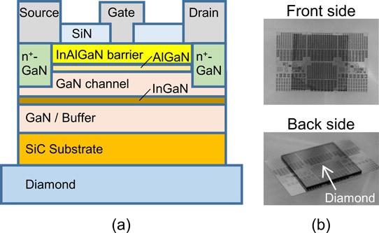
The device material was grown on silicon carbide using metal-organic vapor phase epitaxy (MOVPE). The heterostructure featured an InGaN back barrier aimed at reducing drain current leakage. The top InAlGaN top barrier was grown on an AlGaN spacer in an effort to reduce interface roughness for improved electron mobility in the GaN channel.

Figure 1: (a) Schematic cross-sectional view and (b) photographs of InAlGaN/GaN HEMT on SiC substrate bonded to diamond (9mmx9mm) heat spreader by surface-activated bonding.
Including indium in the top barrier material allows reduced sheet resistance in the channel without increasing tensile strain in the structure, as is inevitable with AlGaN top barriers. The Fujitsu team reports that it has previously used InAlGaN barriers to achieve higher output density than for AlGaN/GaN HEMTs in the W-band range (75-110GHz).
W-band frequencies are allocated for satellite communications, millimeter-wave radar research, military radar targeting and tracking, and automotive cruise control radar. S-band (2-4GHz) applications also include radar, along with a number of local wireless communication devices (WiFi, Bluetooth, etc).
The source/drain contacts consisted of regrown n+-GaN and titanium/gold electrodes. The Schottky gate was nickel/gold. After thinning the SiC growth substrate to 50μm and smoothing with chemical mechanical polishing, the device was bonded to diamond.
The interface between the SiC and diamond was made more thermally conductive by preparing the bond surfaces with argon beam treatment to remove contamination and activate the bond surfaces. The diamond surface also incorporated a thin metal layer that was applied before the argon exposure.
The researchers comment: “This process greatly improves the bonding strength between the SiC and diamond substrates because the formation of the low-density damaged layer on diamond surface is suppressed.”
Optical microscope inspection of the bond could not find any voids. Mechanically peeling apart the device and diamond materials was difficult. These features suggest a strong bond with low thermal resistance.
A HEMT with 0.25μmx50μm gate achieved a maximum drain current of 1058mA/mm and 488mS/mm peak transconductance. Three-terminal hard breakdown in pinch-off came at 257V. The researchers believe the high breakdown voltage was a result of the high growth temperature of the InAlGaN barrier layer, giving higher crystal quality than in InAlN barriers. The researchers report that the breakdown was comparable to what they have achieved with AlGaN/GaN HEMTs fabricated in the same way.
Thermal properties were assessed with an infrared camera. The device temperature reached 120°C with 12W input power on a diamond heat spreader. By contrast, without the diamond heat management it took only 4W to exceed 120°C. Thermal resistance around 100°C was 7.2°C/W for the HEMT on diamond, but this increased to 18.8°C/W without the heat spreader.
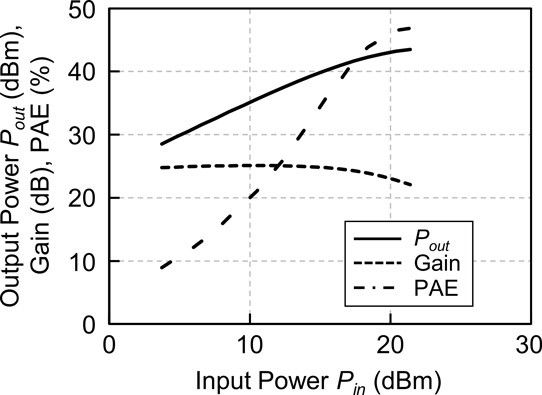
S-band microwave load-pull measurements around 3GHz demonstrated saturated output power of 19.8W/mm with a 1mm total gate width on diamond with 10% duty cycle of 10μs pulses. Without diamond, the power reached only 14.8W/mm. With a 1% duty cycle, the power on diamond increased to 22.3W/mm (Figure 2). The 1% duty cycle power-added efficiency (PAE) was calculated at 47% and the linear gain was 25.1dB.

Figure 2: Power characteristics of InAlGaN/GaN HEMTs with diamond heat spreader evaluated by load-pull measurement under 1%-pulse condition at S-band.
The researchers point out that their work was limited by the maximum voltage of the measuring equipment and that higher drain biases (more than 100V) could give even better
results. However, significant thermal degradation was seen with 10% duty cycle pulses for the HEMT on diamond – 10% duty cycles are common in radar and wireless communication devices.
Since the device does not presently use advanced field control structures, the team hopes that improvements could come from “modulating the potential between the gate and drain electrode and decreasing the magnitude of the electric field at the gate edge”. Presumably, future performance targets would include the 40W/mm power density achieved so far by S-band AlGaN/GaN HEMTs.
We has been focusing on the r&d and production of diamond material, now has a wafer level diamond, diamond heat sink, metal and other related products and services, and after years of precipitation technology, led by basic research and breakthrough progress, obtain head companies such as communications, semiconductor lasers, military industry recognition.
 闽ICP备2021005558号-1
Leave A Message