Pos:
Home NewsCompany ProfileHuge Breakthrough: Peking University Lower Barriers to Growing GaN-on-Si With CSMH AlN Film SolutionTo date, GaN is rapidly emerging both in power and RF applications, thanks to its excellent performance in high-power, high-frequency environments. With the low-cost advantages of large-sized silicon (Si) substrates and compatibility with existing CMOS processes, GaN-on-Si has become the mainstream of the market.
For the epitaxy of GaN-on-Si, if the epitaxy of GaN is performed directly on the surface of the silicon wafer, Si will react chemically with Ga to form a melt-back effect. A layer of AIN film is grown on top to avoid this phenomenon. At the same time, AlN and GaN have very close lattice constants and thermal expansion coefficients, which can reduce the stress problem caused by lattice mismatch. Therefore, a high-quality AlN seed layer is crucial for epitaxial GaN.
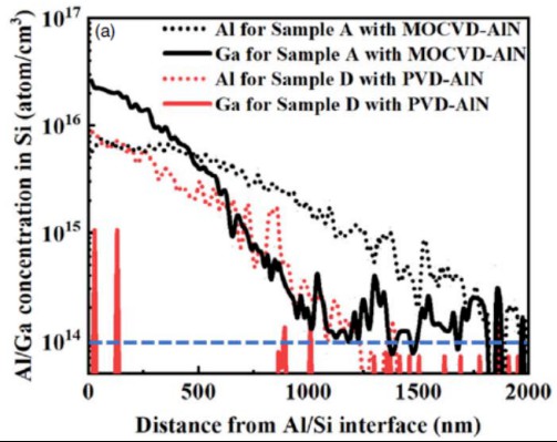
However, if growing the AlN seed layer with the MOCVD method, the residual gallium atoms in the device cavity will diffuse into the high-resistance silicon, resulting in radio frequency loss, which hurts the power gain and power output of the GaN-on-Si radio frequency device. To solve this problem, AlN produced with the PVD physical vapor deposition method can effectively prevent the occurrence of the Ga-Si melt-back phenomenon. Anyhow, obtaining high-quality and crack-free GaN layers on Si substrates with sputtered AIN is a key challenge.
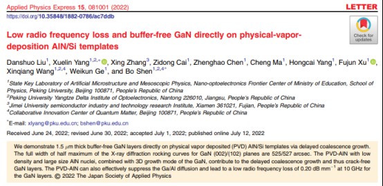
Recently, the research group of Shen Bo and Yang Xuelin of the Wide Bandgap Semiconductor Research Center of the School of Physics, Peking University has succeed in growing a 1.5 μm-thick crack-free GaN layer on the AlN/Si template produced by CSMH. Comparable to conventional GaN growth on Si substrates with complex buffers. More importantly, the PVD-AlN can also effectively suppress the Ga/Al diffusion and lead to a low radio frequency loss of 0.20 dB mm−1 at 10 GHz for the GaN layers.

(a) Al and Ga concentration profiles in the Si substrates for the samples with PVD-AlN and MOCVD-AlN. The detection limit is ∼1014 cm−3, which is marked with a dotted line.

(b) RF loss for the GaN layers grown on the PVD-AlN and MOCVD-AlN.
CSMH utilized PVD physical vapor deposition process to produce a high-quality AlN seed layer, which lays a good foundation for the effective growth of high-quality GaN and significantly reduces the RF loss at the same time. This important research result, entitled "Low radio frequency loss and buffer-free GaN directly on physical-vapor-deposition AlN/Si templates", is published in the journal Applied Physics Express. The first author of the paper is Liu Danshuo, a doctoral student at Peking University. The co-authors are Professor Shen Bo and Professor Yang Xuelin of Peking University, and Zhang Xing, the co-founder/CEO of CSMH.
APEX reviewer commented, "This paper reports a growth process using sputtered AlN to solve the problems of low throughput and diffusion of Ga and Al into Si substrates when fabricating GaN/AlN/Si structures by MOCVD. By controlling the surface morphology of sputtered AlN and lowering the coalescence rate of GaN grains, the authors have succeeded in growing crack-free thick GaN films. The paper adequately points out the problems of previous studies on the growth of GaN on Si substrates and solves them with a new growth method. I believe this paper is worthy of publication in APEX."
Learn more about the paper: https://iopscience.iop.org/article/10.35848/1882-0786/ac7ddb

CSMH is a joint venture company based on cutting-edge semiconductor manufacturing technologies with investments from Korea, China, and Singapore. We are equipped with advanced semiconductor production equipment to produce high-quality Diamond wafers, Diamond heat sinks and AlN templates on a variety of substrates, including AlN on Sapphire, AlN on Diamond, and AlN on Si. Our product's performance has improved to a level that is among the best in the world.

Check out the bullet features of AlN on Si:
l XRC<0.8°;
l The surface roughness Ra<1.5nm;
l Assist to grow high-quality GaN epitaxial wafer with lower cost;
l More conducive to mass production.
Based on the accumulation of AlN thin film technology for many years, CSMH will offer our customers products of high quality and reliable performance while contributing to the rapid development of BAW filters, sensors, and other application fields in the future.

 闽ICP备2021005558号-1
Leave A Message